


Bump Fusion
Applied for precision packaging scenarios of high‑performance computing chips, 3D stacked ICs and high‑end RF chips.
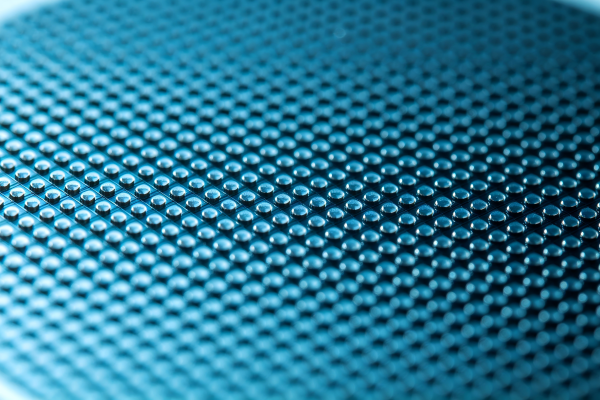
Bump Fusion is the core process for wafer bump formation. High‑temperature reflow enables uniform shaping of metallic bumps on the wafer surface to build high‑density vertical interconnection contacts.
The adoption of well‑matched dedicated solders ensures uniform bump dimensions and smooth bump surfaces, laying a reliable interconnection foundation for flip‑chip and 2.5D stacked applications.
Industry Challenges & Solutions
Conventional bump solders tend to suffer from inconsistent bump size, surface oxidation, voids and collapse after reflow. Poor coplanarity will directly trigger subsequent flip‑chip cold solder joints and conduction failure.
Huaqing’s customized alloy solders dedicated to wafer bumps feature controllable melt flowability and high reflow forming consistency. They deliver low surface oxidation of bumps and ultra‑low void rates with excellent bump coplanarity. Compatible with batch reflow processes for full‑size wafers, the solders greatly improve yield and long‑term electrical reliability for high‑end advanced packaging.
Related Products
Quickly browse products and applications. VisitProduct Centerfor matching inquiries.



 Follow Us
