

2.5D&3D
Serving cutting‑edge technology fields including high‑performance computing, artificial intelligence, mobile terminals and data centers.

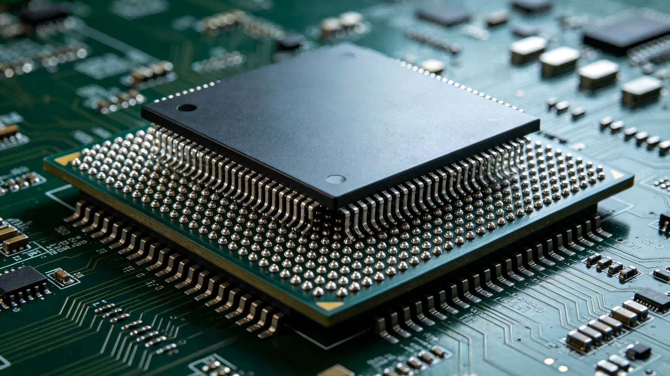
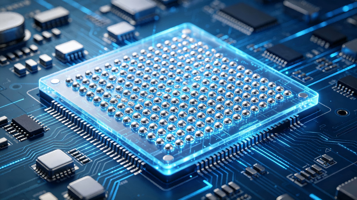
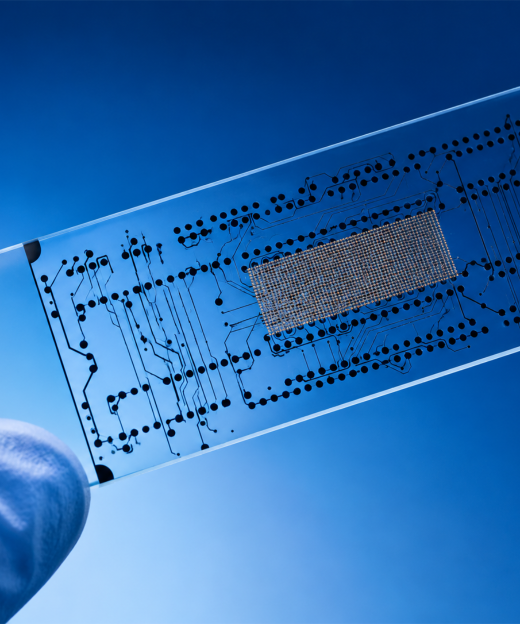
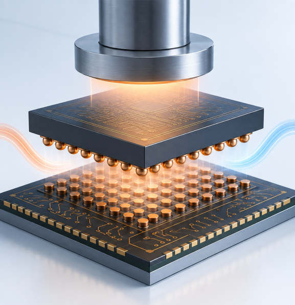
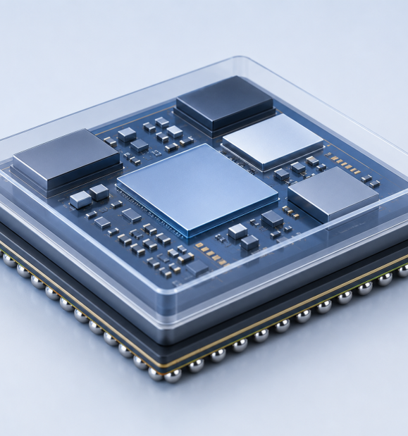
2.5D/3D IC realizes vertical stacking or horizontal interconnection of chips through Through‑Silicon Vias (TSV) and interposers. It aims to break through the bottleneck of Moore’s Law, drastically boosting chip integration and bandwidth while reducing power consumption. Its core lies in achieving reliable interconnection and efficient heat dissipation between individual chip layers.
Industry Challenges & Solutions
The biggest challenge for 2.5D/3D IC packaging lies in realizing high‑density, void‑free and reliable soldering within an extremely compact space. Meanwhile, it is essential to address complex thermal‑stress issues induced by multi‑layer structures and differences in thermal‑expansion coefficients of dissimilar materials.
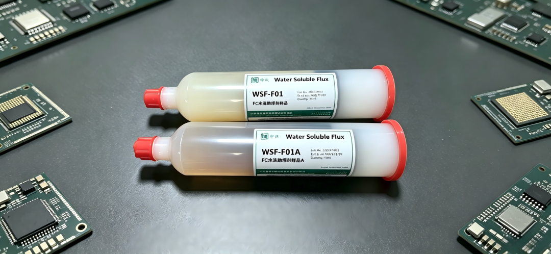
Targeting the unique requirements of 2.5D/3D IC, Huaqing electronic materials deliver customized high‑performance solders and process solutions. Featuring outstanding wettability and flowability, our solders can effectively fill micro‑gaps and achieve low‑void soldering. Furthermore, by optimizing alloy compositions and microstructures of solders, thermal stress generated during packaging can be efficiently mitigated. This greatly improves yield and long‑term reliability for 2.5D/3D IC packaging, and provides solid material support for customers’ next‑generation chip designs.
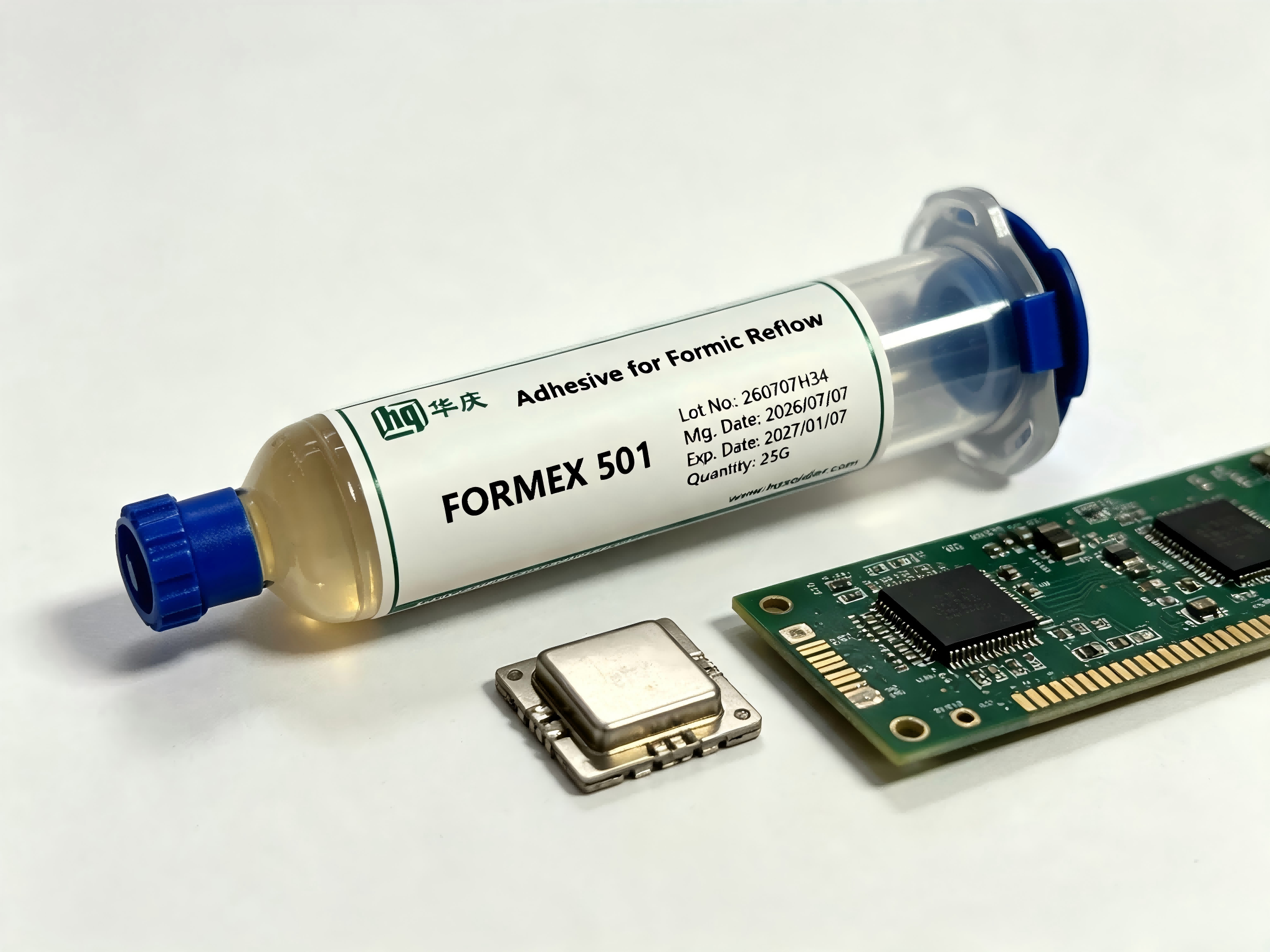
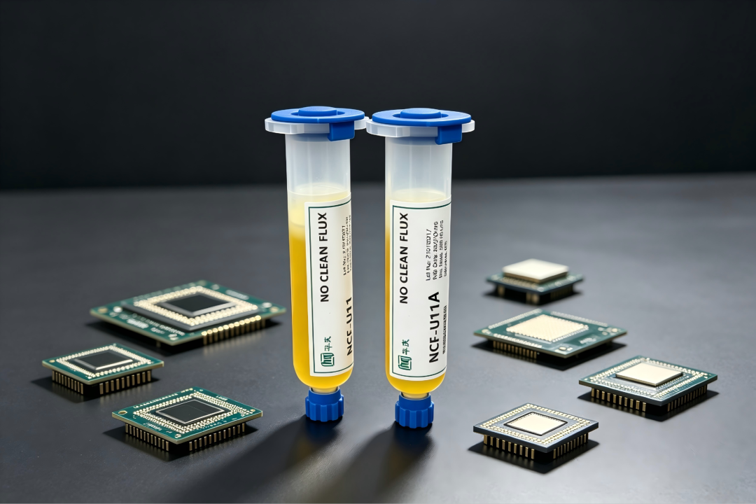
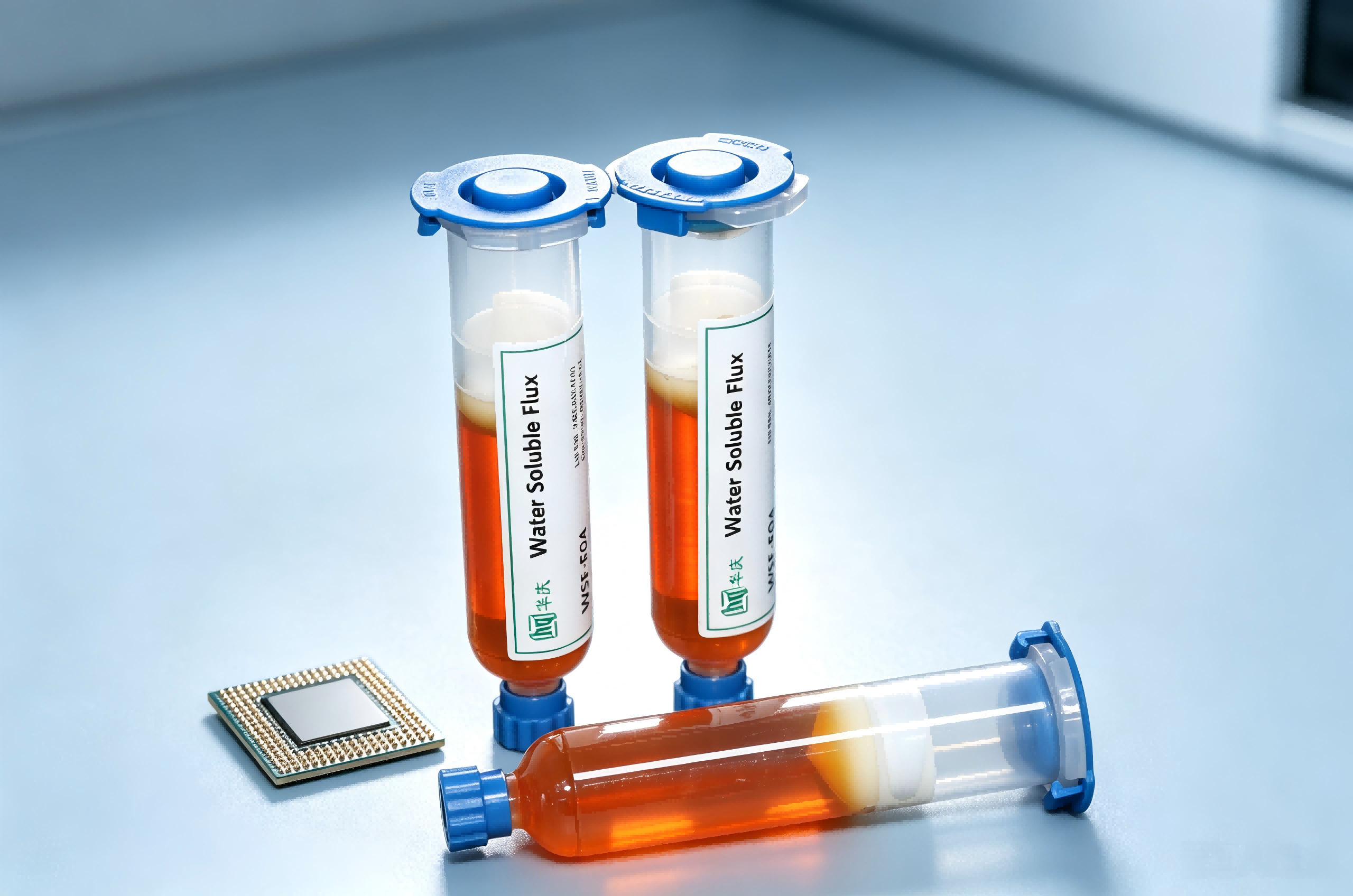
Related Products
Quickly browse products and applications. VisitProduct Centerfor matching inquiries.
Related Applications


 Follow Us
