

Overview
Whether for new‑product verification of wafer bumping, production‑line yield optimization, or adaptation to upgrading trends in advanced packaging and high‑end chip sectors, Huaqing’s technical team and customized supporting materials can achieve precise scenario‑oriented matching. We help customers break through technical bottlenecks and realize dual improvement in performance and production capacity.
Core Value
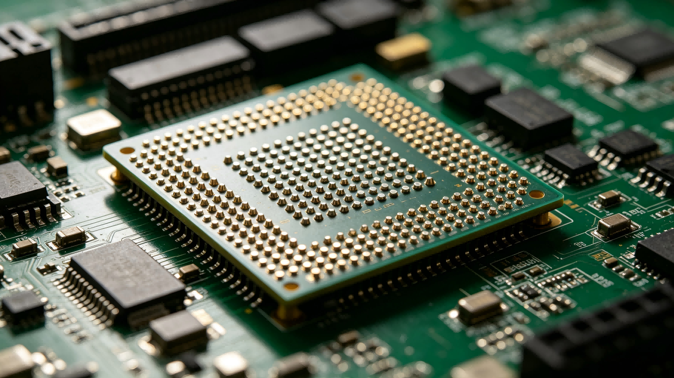
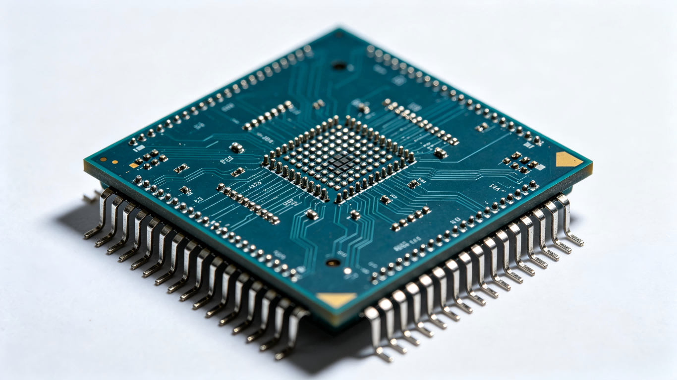
Wafer bumping serves as the core interconnection component for semiconductor advanced packaging, especially flip‑chip technology. Acting as a “micro‑bridge” between chips and substrates, it undertakes critical functions of electrical connection and mechanical fixation. It directly determines chip packaging density, signal‑transmission efficiency and operational reliability, and is widely applied in high‑end processors, memories, RF chips, image sensors and other fields.
With in‑depth focus on supporting materials for wafer bumping, Huaqing precisely meets requirements for micron‑level accuracy and high reliability. Premium materials and professional technologies consolidate the core competitiveness of customers’ products.
Core Significance
Supporting materials form the fundamental basis for wafer bumping to deliver core performance. Their quality directly governs interconnection performance and long‑term reliability of bumps.
Suitable supporting materials for bump soldering and UBM (Under‑Bump Metallurgy) layers can precisely satisfy micron‑level forming requirements, enhance adhesion between bumps and wafers, block metal inter‑diffusion and mitigate interfacial defects. They guarantee electrical conductivity and structural stability of bumps, lay a solid foundation for efficient and stable chip operation, and fundamentally reduce packaging‑failure risks and subsequent rework costs.
Industry Challenges
As chips evolve toward higher density, miniaturization and superior performance, the wafer‑bumping industry faces multiple practical challenges
Bump pitch keeps shrinking down to the micron scale, substantially raising requirements for accuracy and uniformity of supporting materials. Conventional materials struggle to satisfy fine‑pitch forming requirements.
Interfacial reliability is difficult to control. Issues such as IMC (Intermetallic Compound) growth, bump voids and bump collapse tend to occur and shorten chip service life.
High‑end supporting materials (e.g. special plating solutions, UBM target materials) are heavily import‑dependent with unstable supply chains. Delayed responses for customized adaptation fail to meet innovation demands of domestic enterprises.
Solutions
Huaqing provides one‑stop wafer‑bumping solutions targeting industry pain points
Self‑developed high‑precision bump‑soldering materials and UBM supporting materials, compatible with fine‑pitch bump forming, improving uniformity and adhesion and reducing interfacial defects.
Deliver customized process guidance to optimize key process parameters such as electroplating and reflow, and resolve challenges including bump collapse and bridging.
Full‑cycle technical follow‑up to precisely fulfill customized requirements for diverse packaging scenarios, helping customers reduce costs, improve efficiency and overcome technical bottlenecks.
Related Applications





 Follow Us
Copyright@ 2026 All Reserved Copyright © Shanghai Huaqing Solder Material Technology Co., Ltd. All Rights Reserved.
Hu‑Wang‑An‑Bei 31011402003768
Hu ICP 2023012058‑1
