

VR11-SS5
It is specially designed for vacuum soldering processes. Vacuum soldering drastically reduces void formation during bonding and improves product reliability, which is critical for thermal assemblies, power devices and DBC soldering applications.
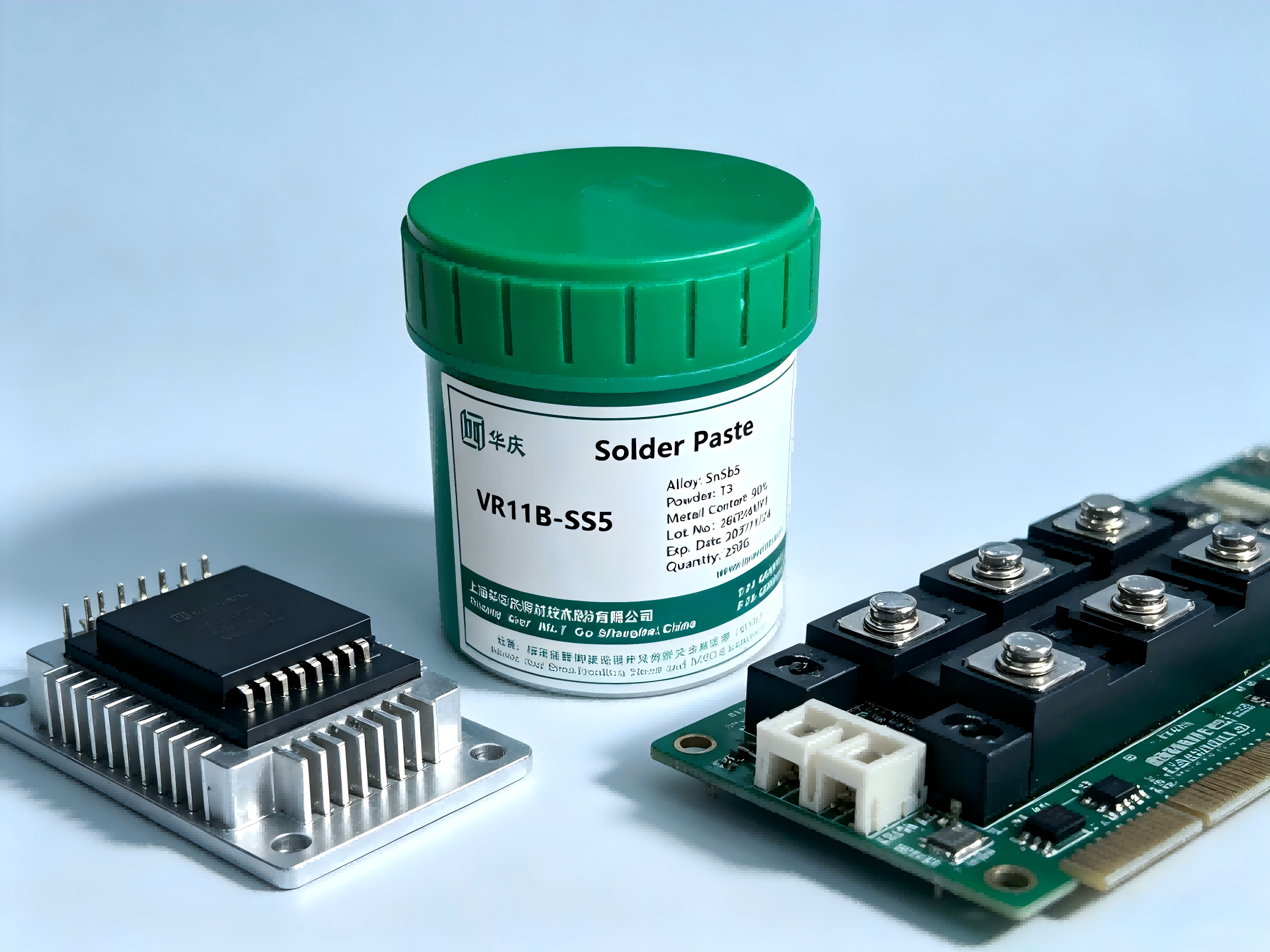
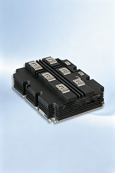
VR11-SS5 features moderate activity, easily cleanable post-soldering residues and non-discoloration of components, making it highly suitable for semiconductor packaging. It is especially ideal for bonding between large-size chips, DBC and heat sinks in power devices such as IGBTs. Products packaged with VR11-SS5 can achieve a void rate below 1%, delivering uniform and flat solder interfaces with minimal spattering and solder balls.
Residues left after VR11-SS5 reflow can be readily removed with common solvent cleaners including hydrocarbons, halocarbons, or water-based cleaners. After cleaning, no discoloration, corrosion or water-like stains remain on chips, DBCs and heat sinks.
The unique formulation of VR11-SS5 effectively suppresses chip or DBC shifting. Even on heat sinks with a large pre-bend curvature, DBC displacement can be prevented to boost soldering yield.
Core Advantages
• Activity grade ROL0
• Low soldering void rate (<1%)
• Outstanding performance in inhibiting chip shifting
• Wide process window, compatible with various heating profiles
• Compatible with all common metallic interfaces: copper, nickel, silver and gold
• Minimal spattering and solder balls
• Easily cleanable residues
• No discoloration on chips, circuits or substrates
Related Products
Quickly browse products and applications. VisitProduct Centerfor matching inquiries.
Related Applications
Market








 Follow Us
