

Semiconductor Advanced Packaging

Semiconductor Advanced Packaging
Overview
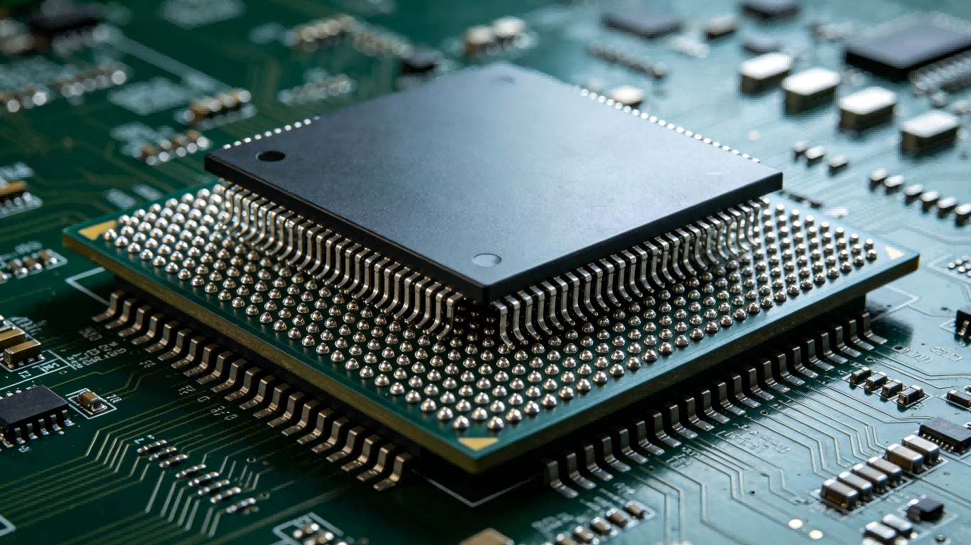
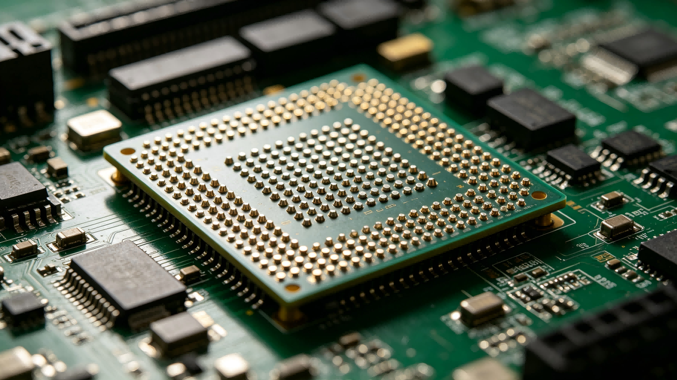
In the post‑Moore era, advanced semiconductor packaging has become a core driving force for chip performance improvement. Technologies such as 2.5D/3D IC, SiP, Flip‑Chip and TCB thermal‑compression bonding are being rapidly industrialized across domestic manufacturing lines, while local material substitution is gathering momentum. This field imposes stringent performance benchmarks for micro‑interconnection, low void formation, minimal thermal stress and long‑term operational reliability.
Core Application Scenarios
AI high‑performance computing chips
Wide‑bandgap power devices including IGBT, SiC and GaN
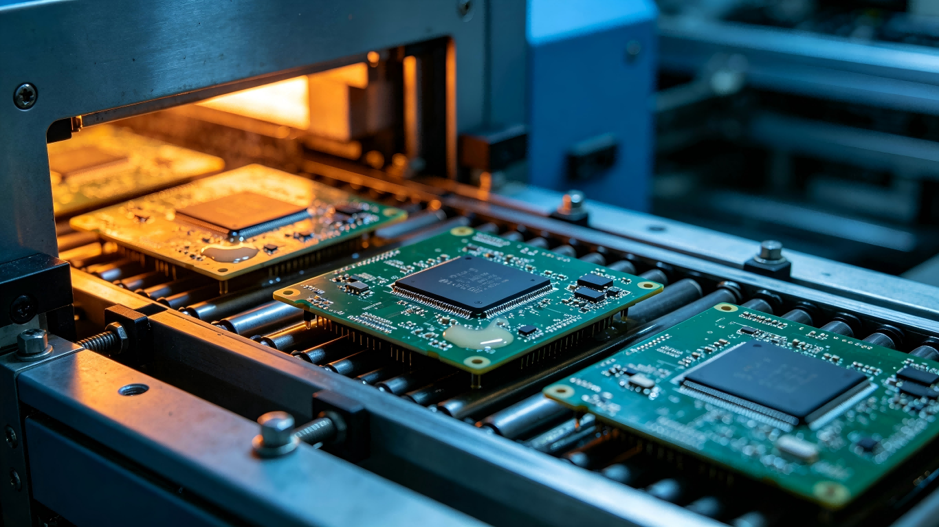
Flip‑Chip & TCB thermal compression bonding processes
Chip die‑attach and shielding frame assembly
Key Technical Challenges
Reliable formation of ultra‑fine micro‑solder joints under miniaturized pitch
Strict control of void ratio and interfacial thermal stress to prevent chip damage
Satisfy multi‑dimensional reliability validation including temperature cycling and power cycling
Maintain ultra‑low ionic residue to mitigate electrochemical migration risks
Solutions
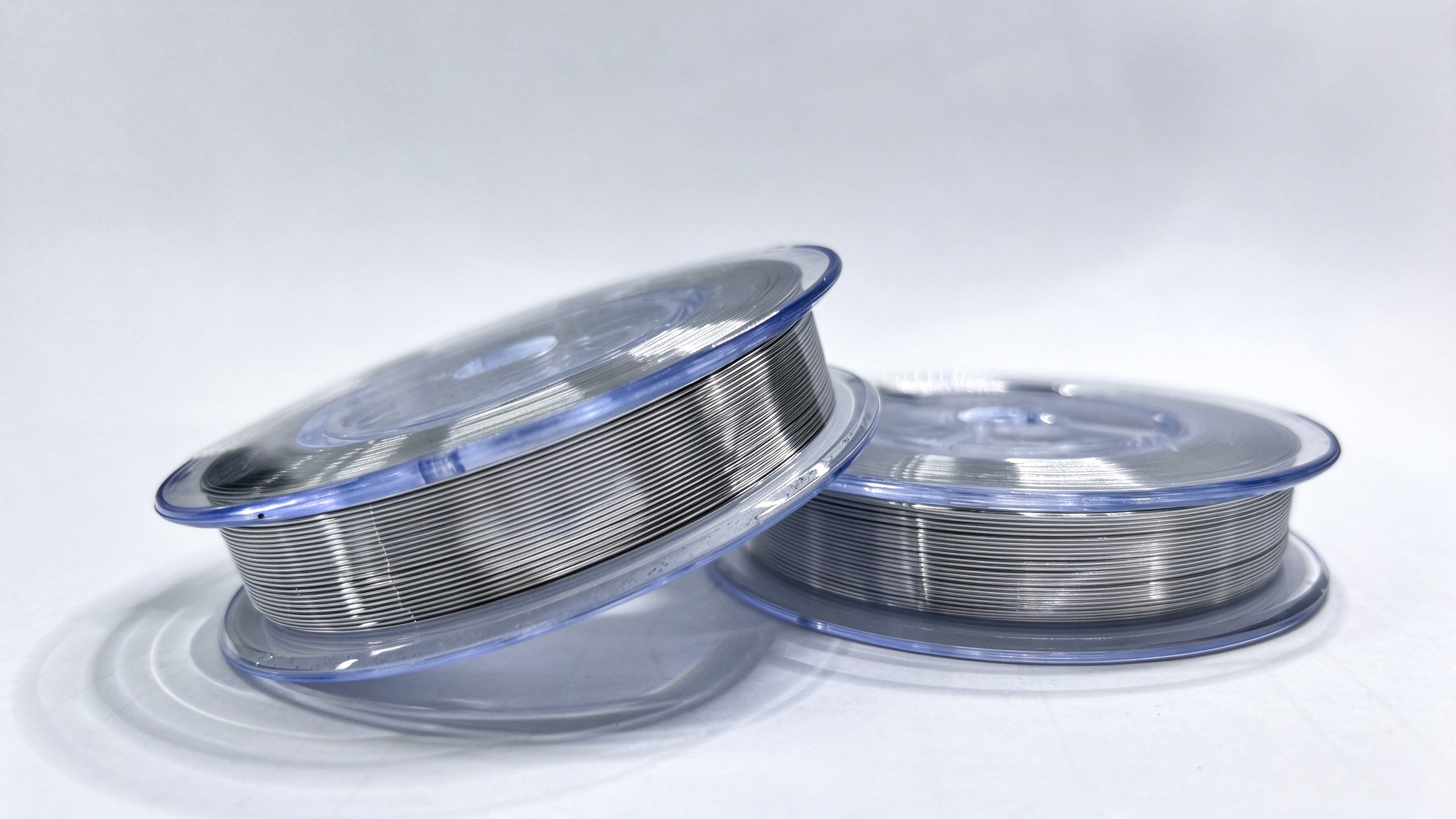
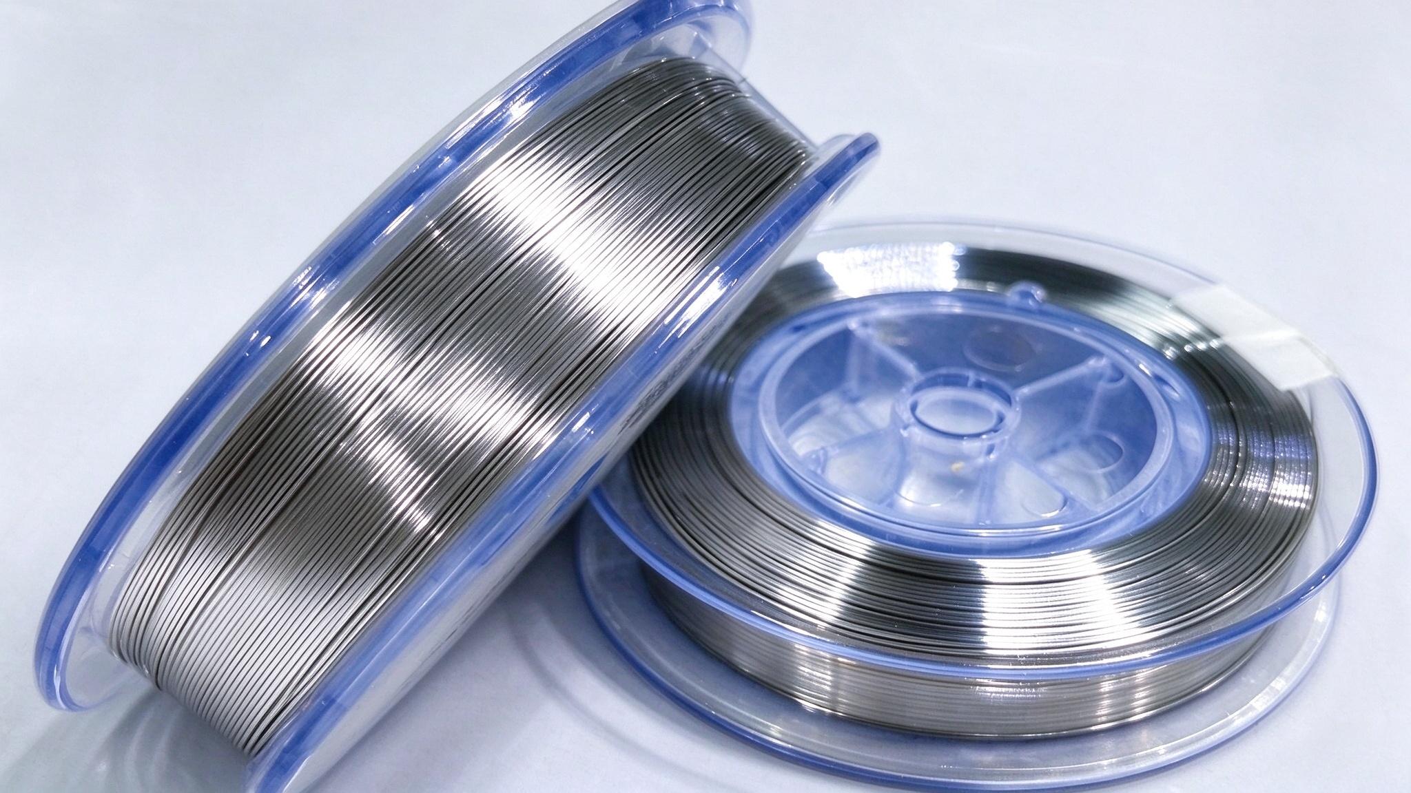
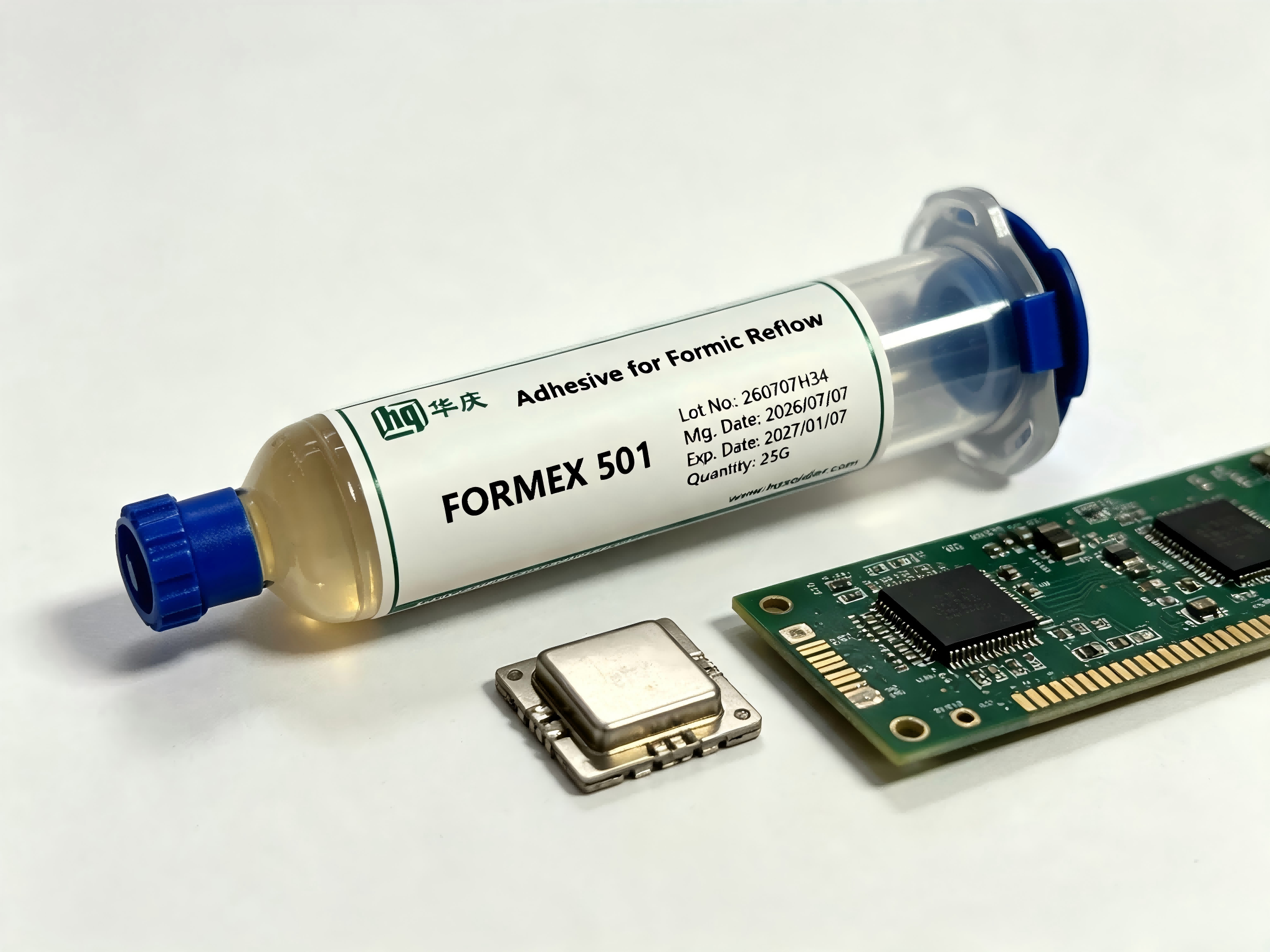
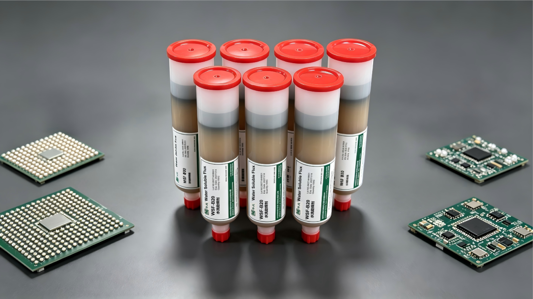
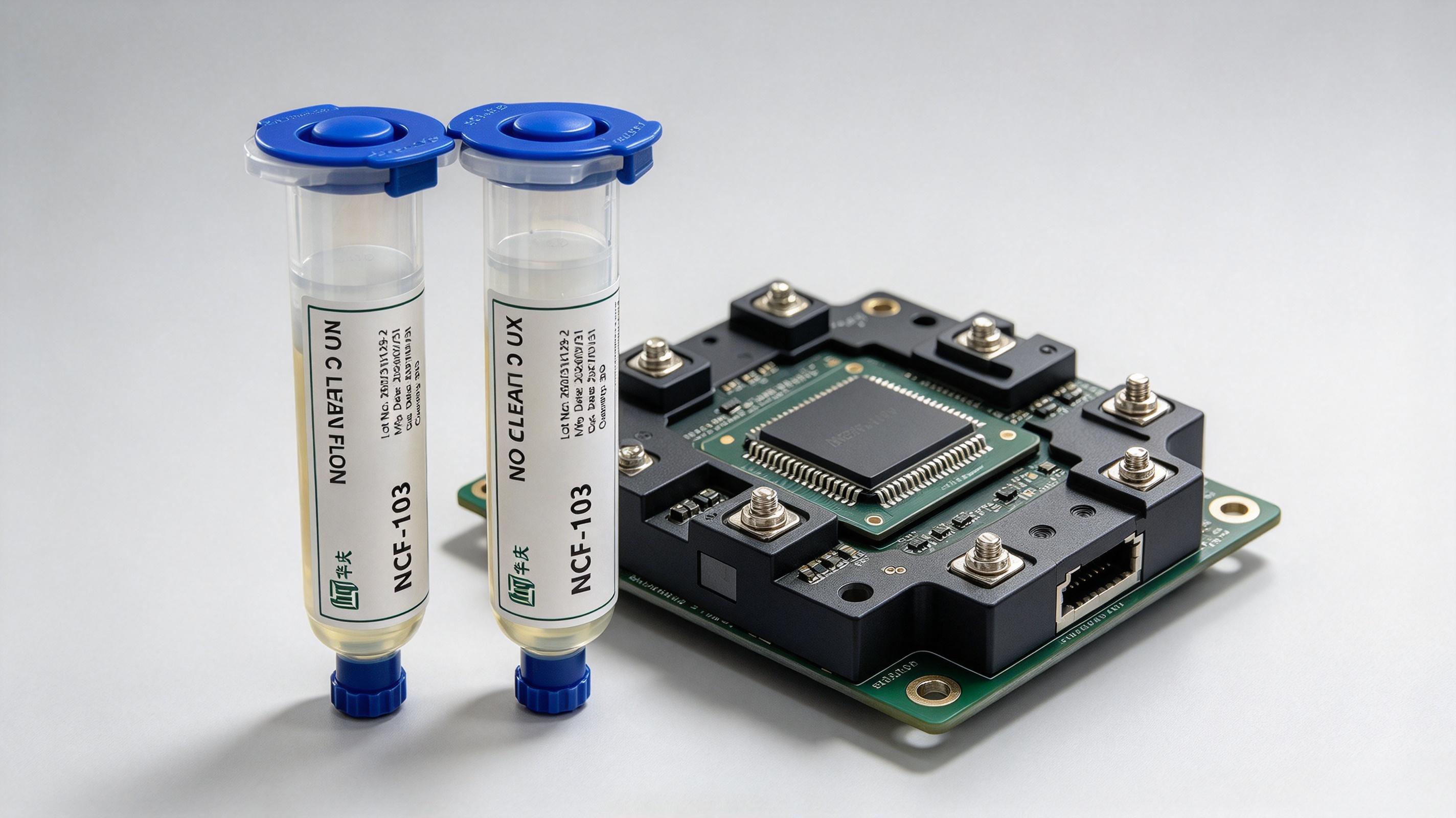
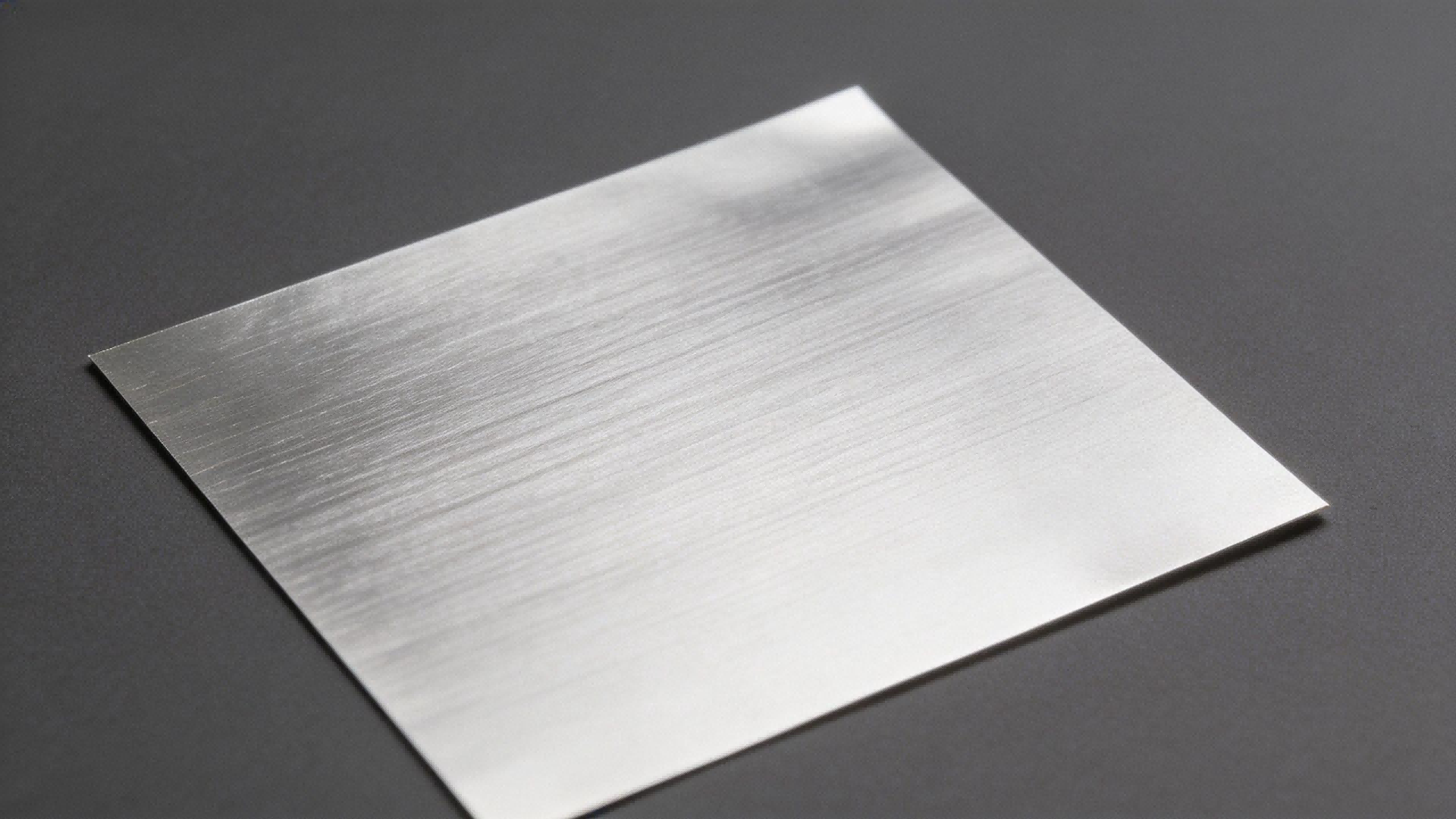
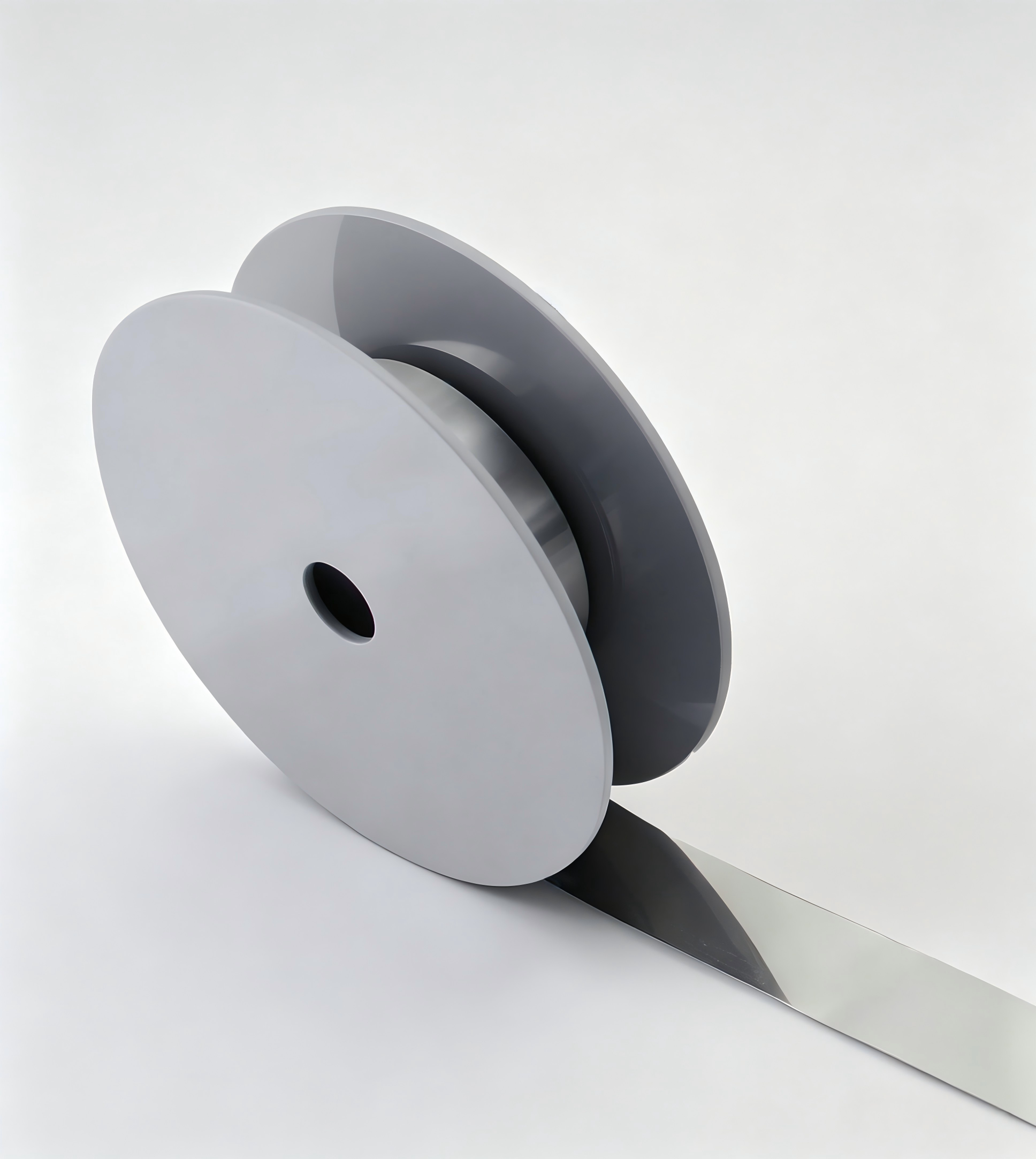
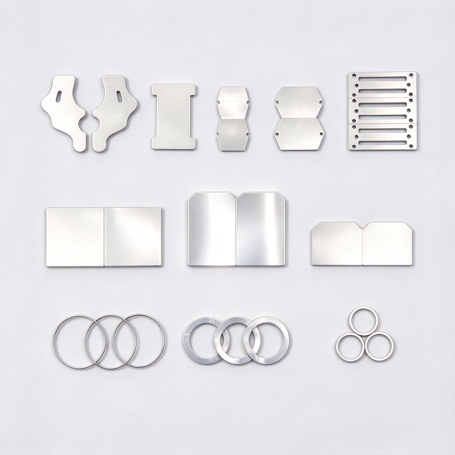
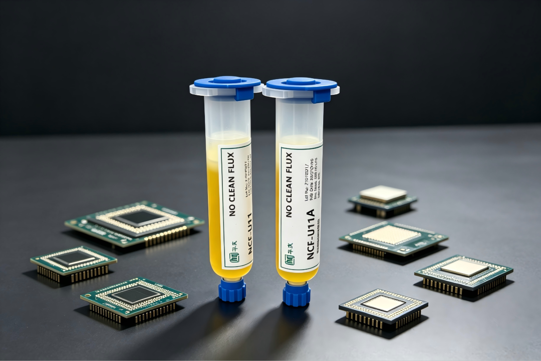
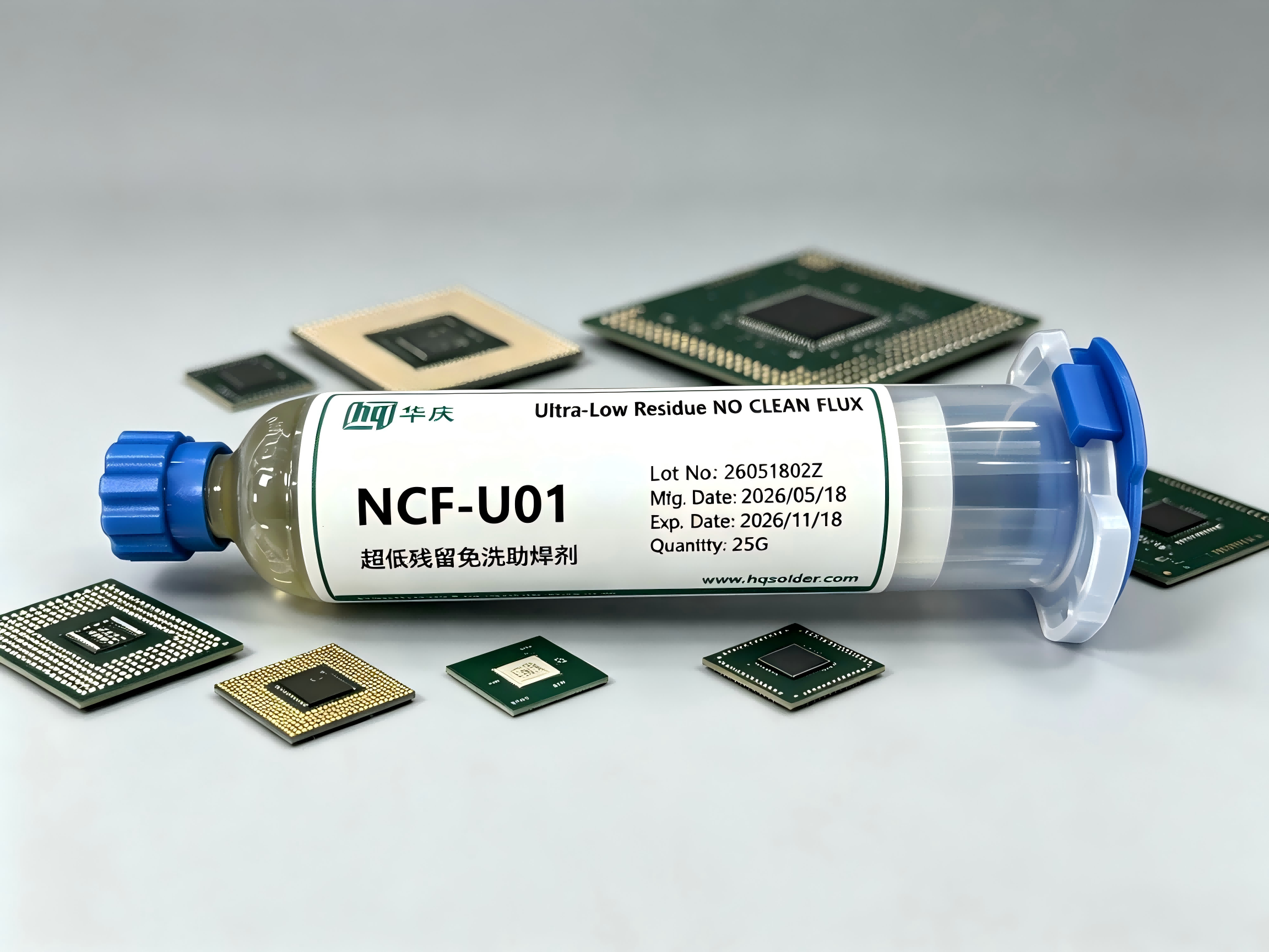
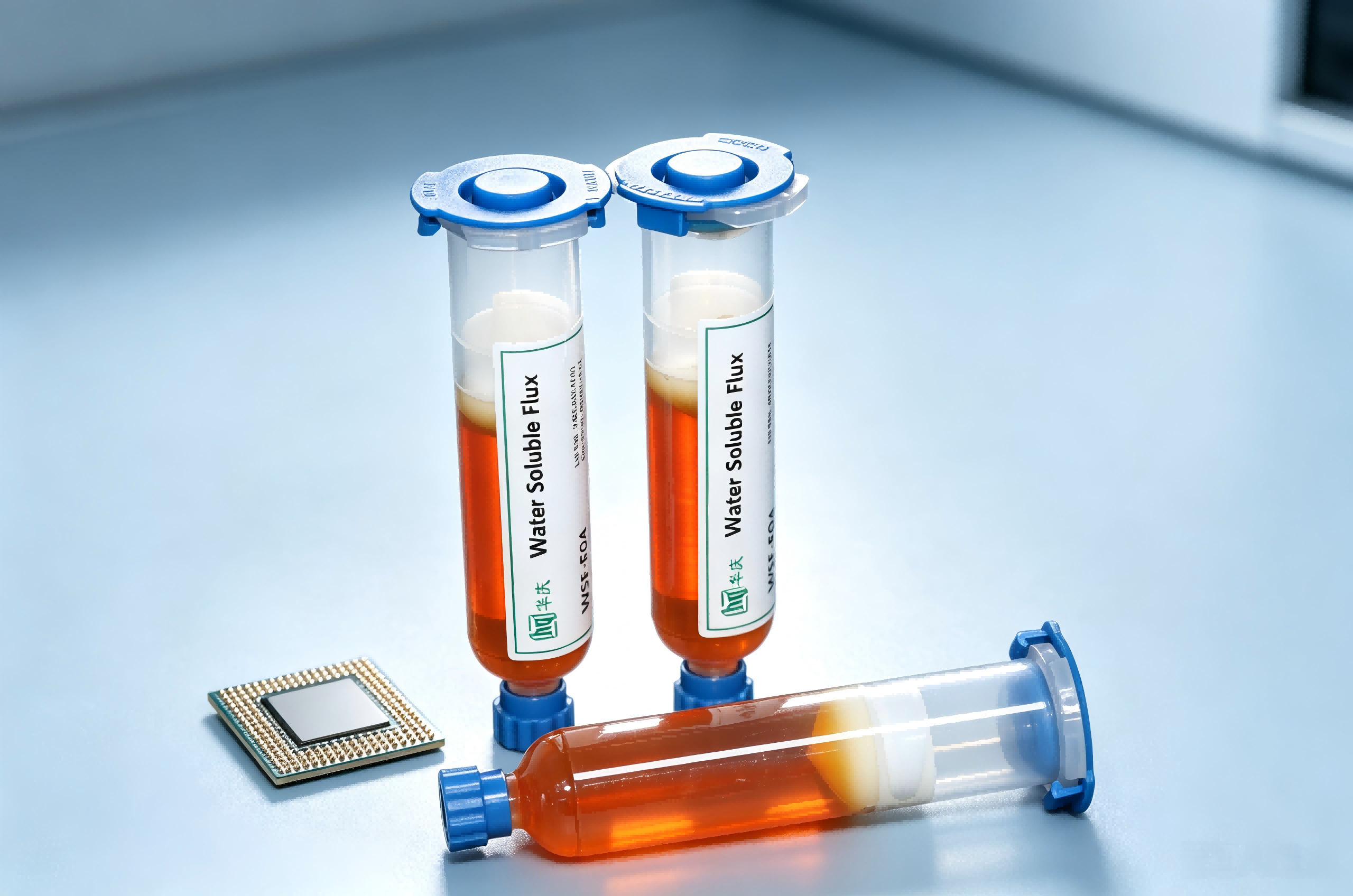
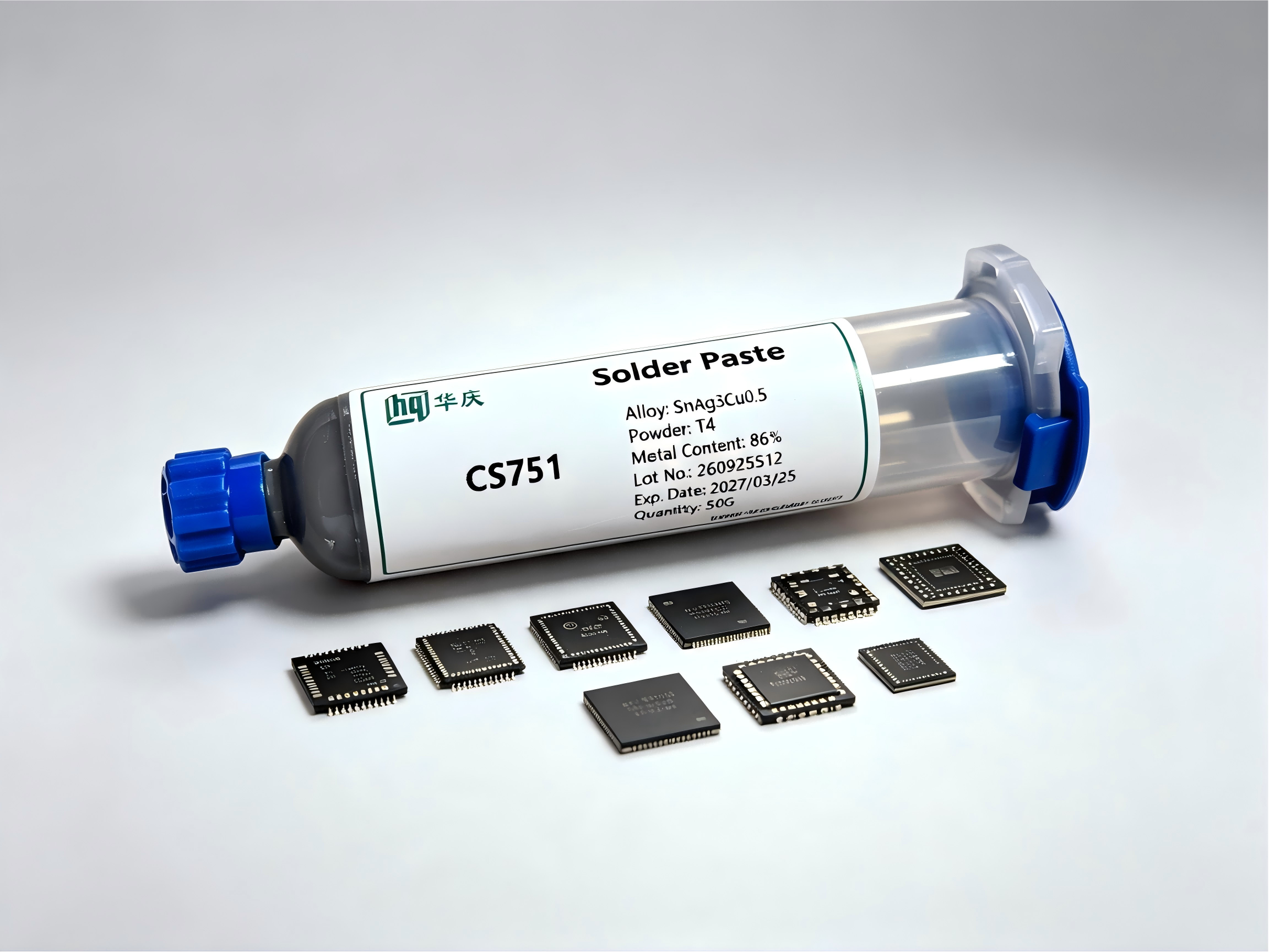
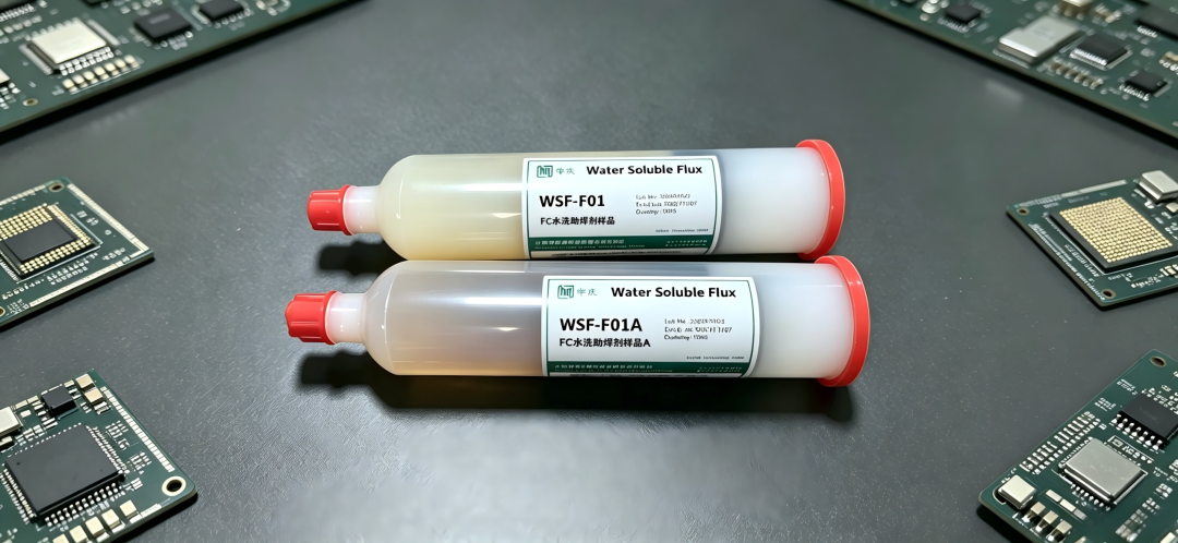
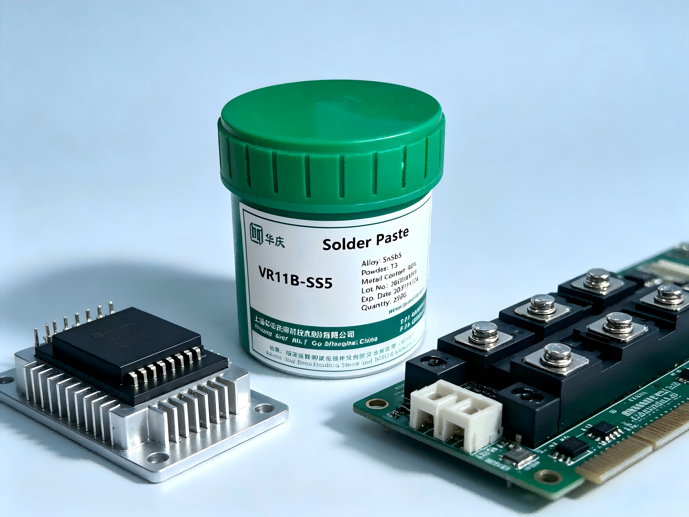
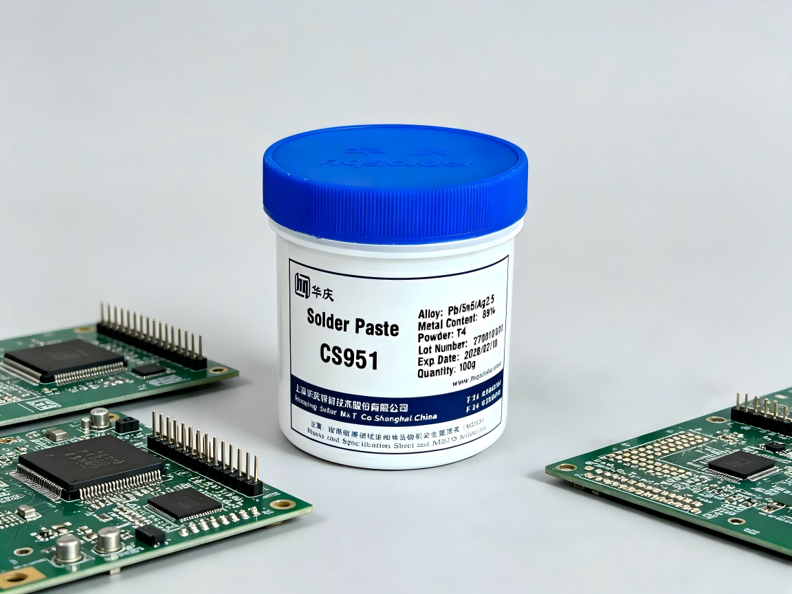
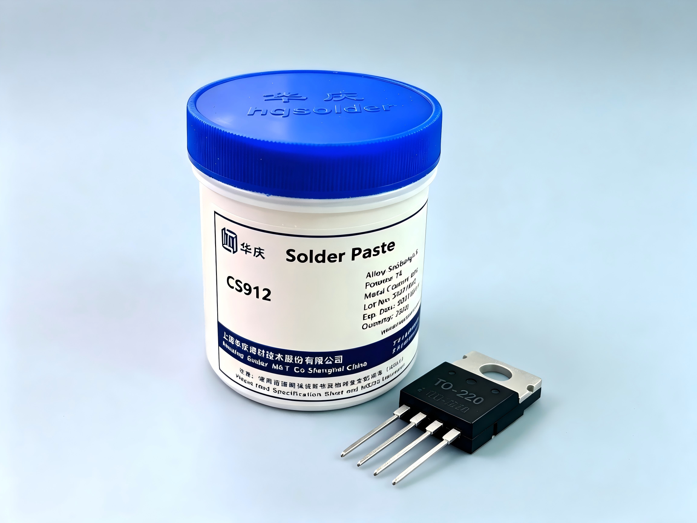
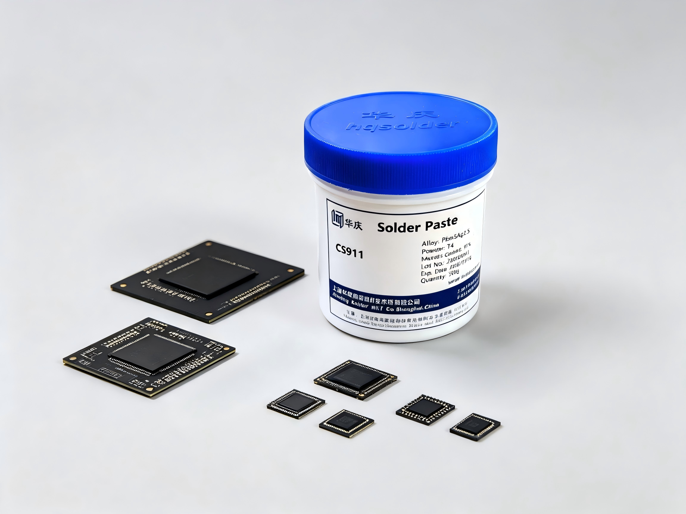
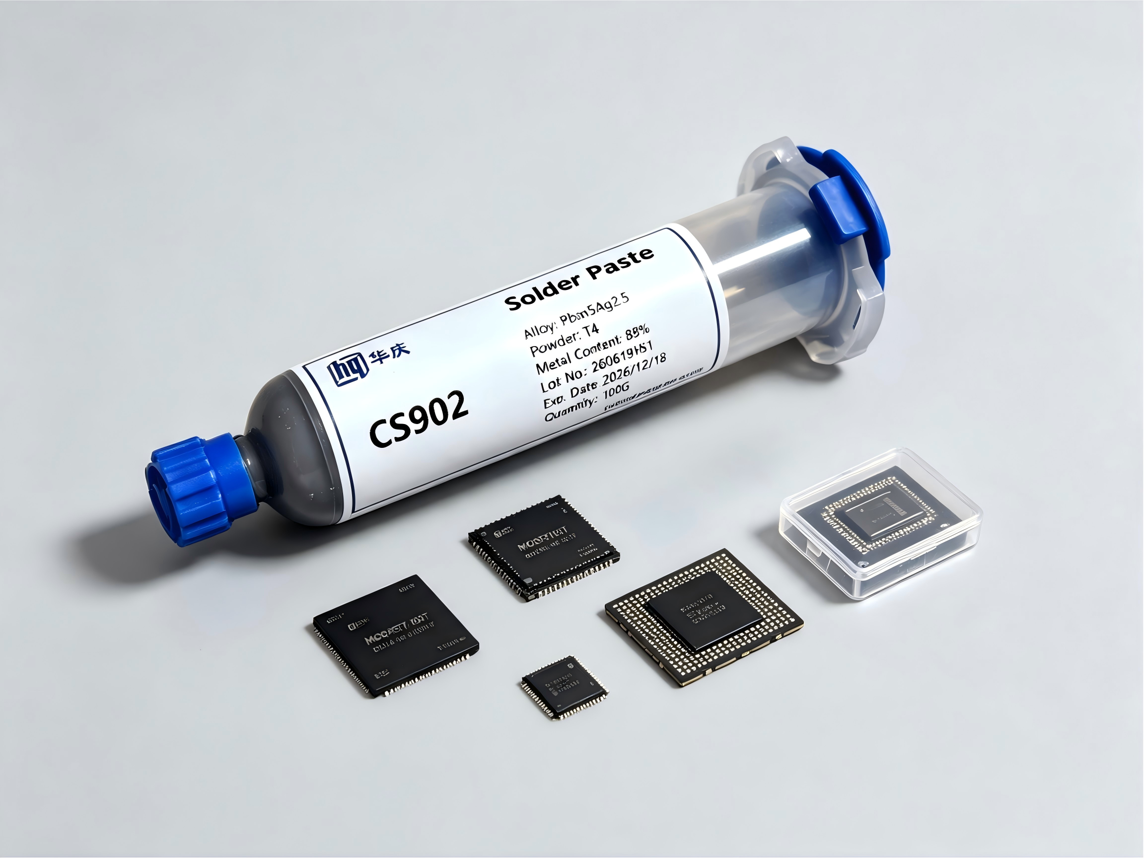
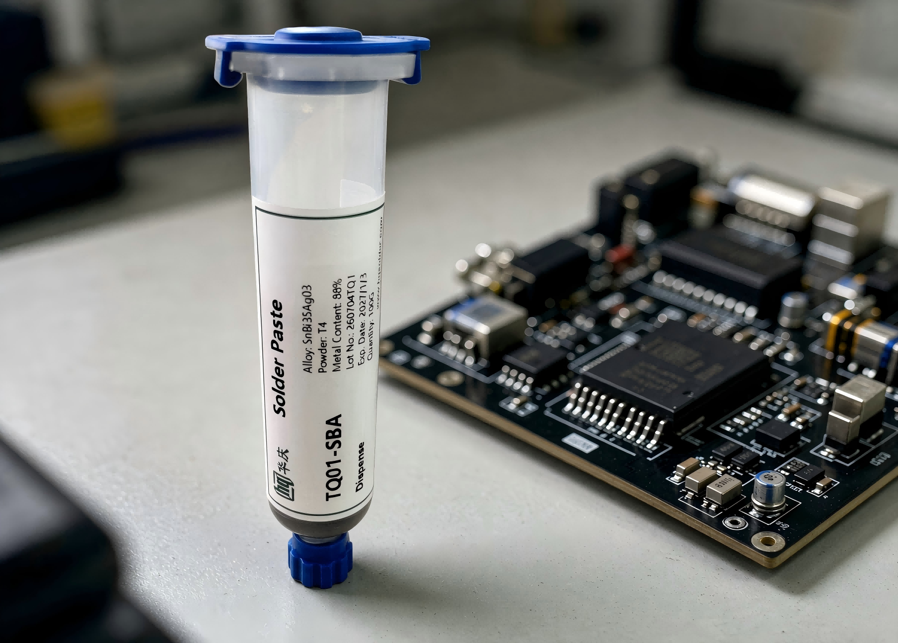
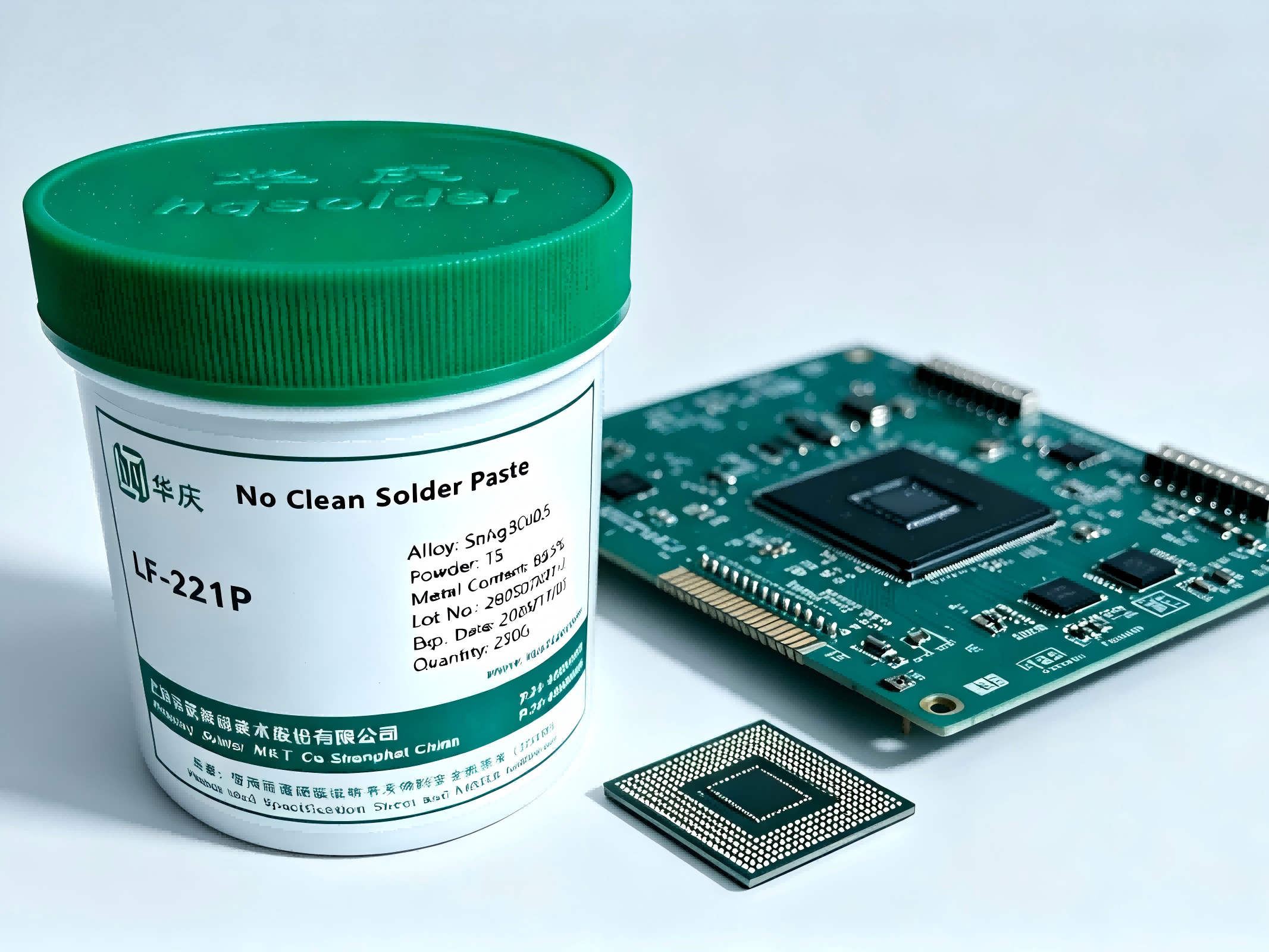
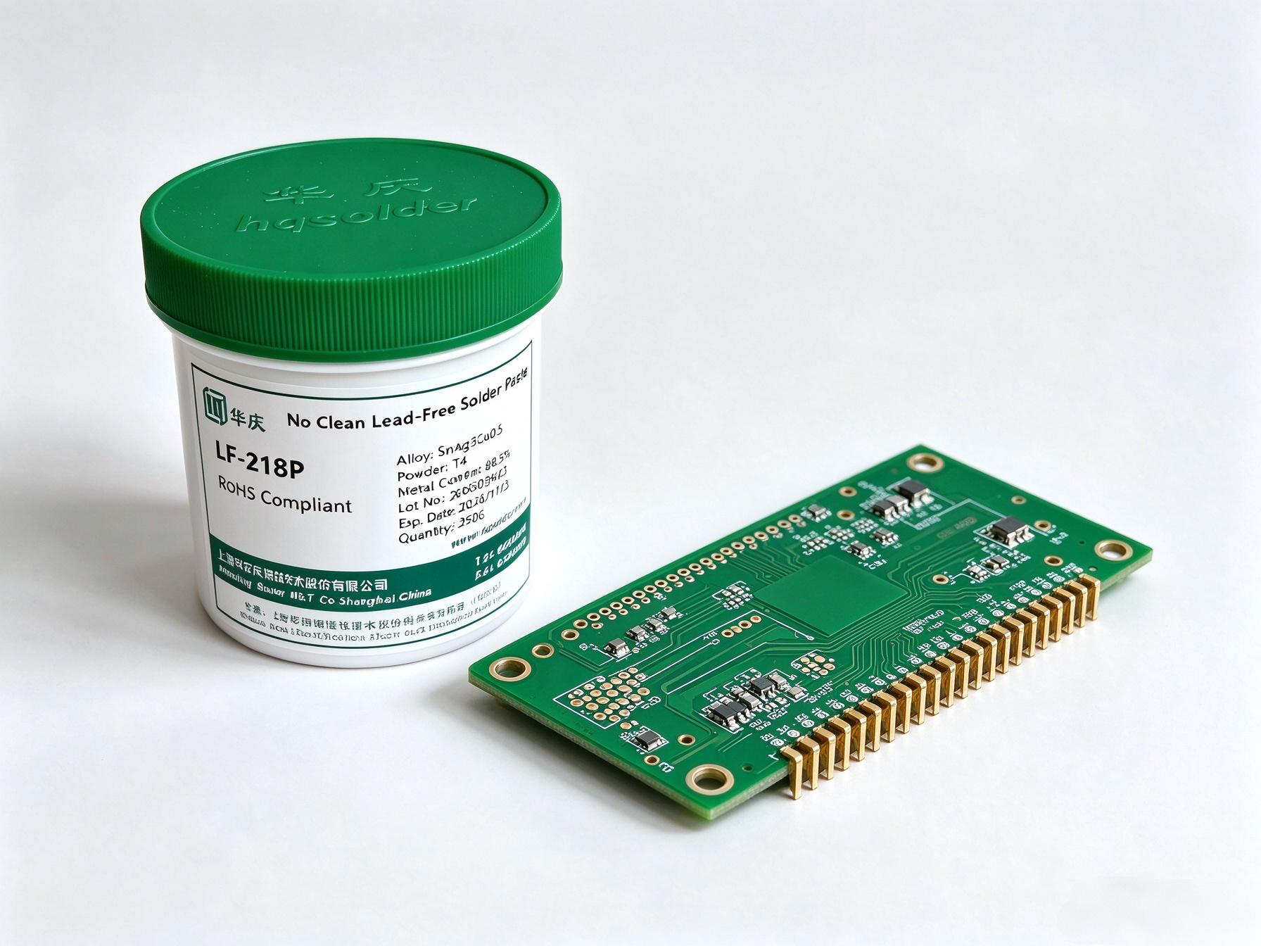
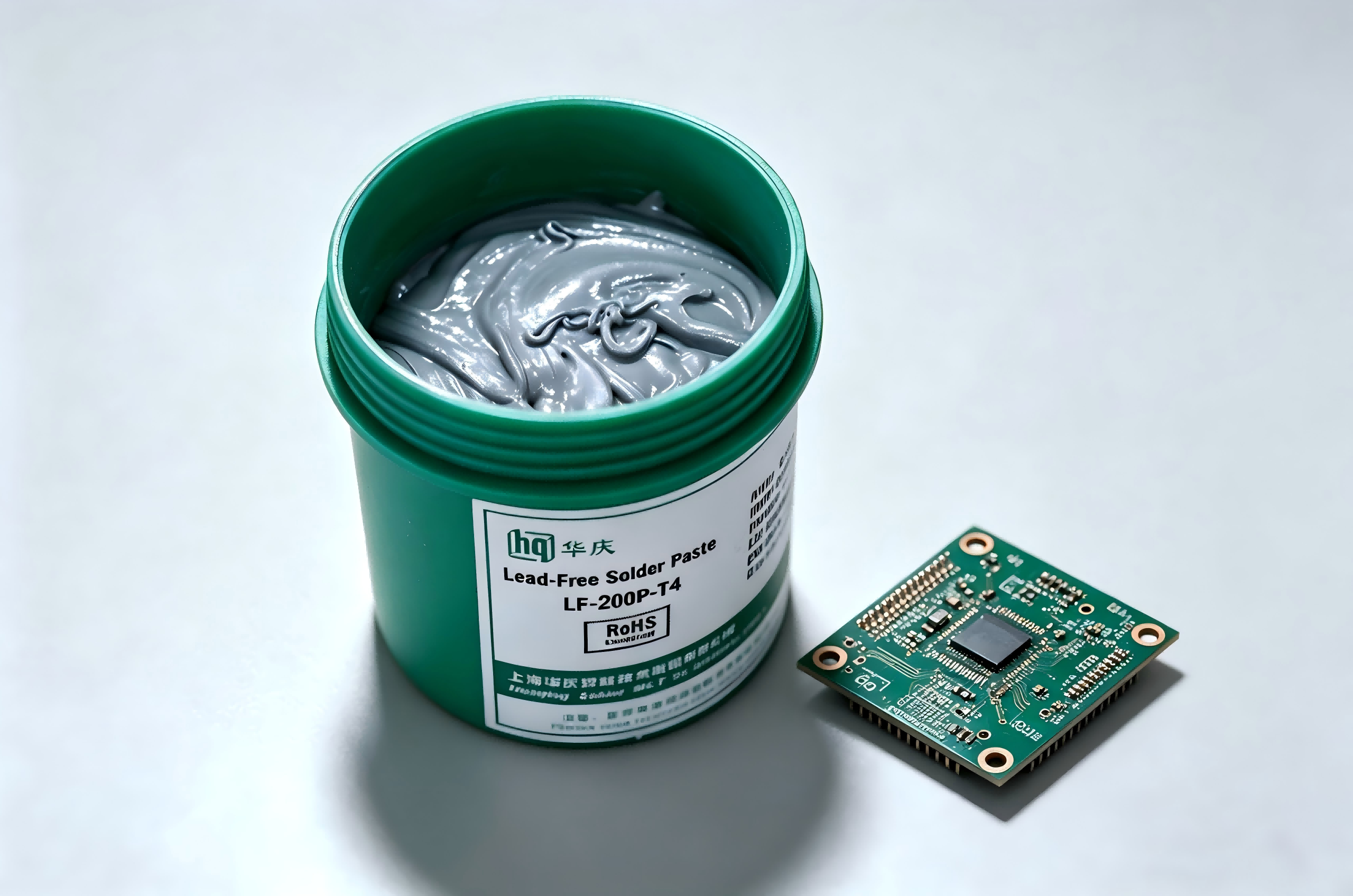
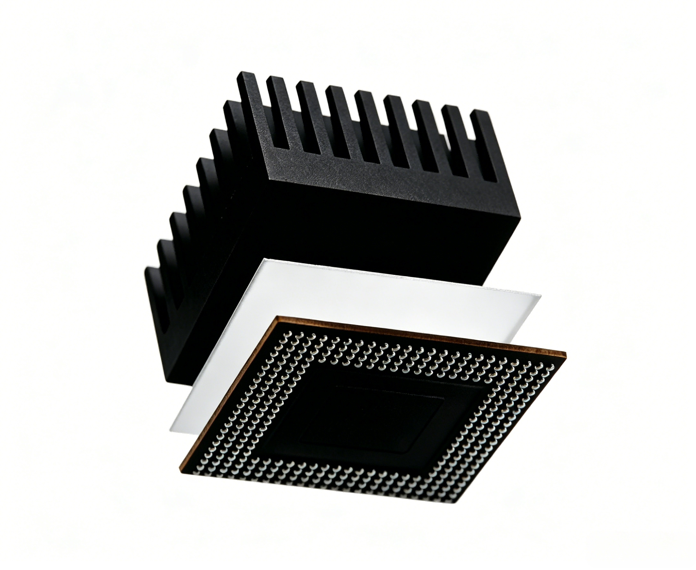
Huaqing provides a complete portfolio of specialized solder pastes, pre‑formed solder foils, TIM thermal interface materials and low‑residue fluxes tailored for advanced packaging processes. Custom‑tuned alloy systems and optimized powder particle distribution deliver superior rheological properties for micro‑printing, thermal compression bonding and vacuum reflow. Our products have passed automotive‑grade reliability qualification, and we offer joint process development and on‑site technical support for packaging manufacturers.
Related Products
Quickly browse products and applications. VisitProduct Centerfor matching inquiries.
Related Applications







 Follow Us
